- 您现在的位置:买卖IC网 > Sheet目录286 > 24FC1026-I/P (Microchip Technology)IC EEPROM 1024KB 1MHZ 8-DIP
24AA1026/24LC1026/24FC1026
1.0
ELECTRICAL CHARACTERISTICS
Absolute Maximum Ratings (?)
V CC .............................................................................................................................................................................6.5V
All inputs and outputs w.r.t. V SS .......................................................................................................... -0.6V to V CC +1.0V
Storage temperature ...............................................................................................................................-65°C to +150°C
Ambient temperature with power applied ................................................................................................-40°C to +125°C
ESD protection on all pins ??????????????????????????????????????????????????????????????????????????????????????????????????????????????????????????????????????????????????????? 4 kV
? NOTICE : Stresses above those listed under “Absolute Maximum Ratings” may cause permanent damage to the
device. This is a stress rating only and functional operation of the device at those or any other conditions above those
indicated in the operational listings of this specification is not implied. Exposure to maximum rating conditions for
extended periods may affect device reliability.
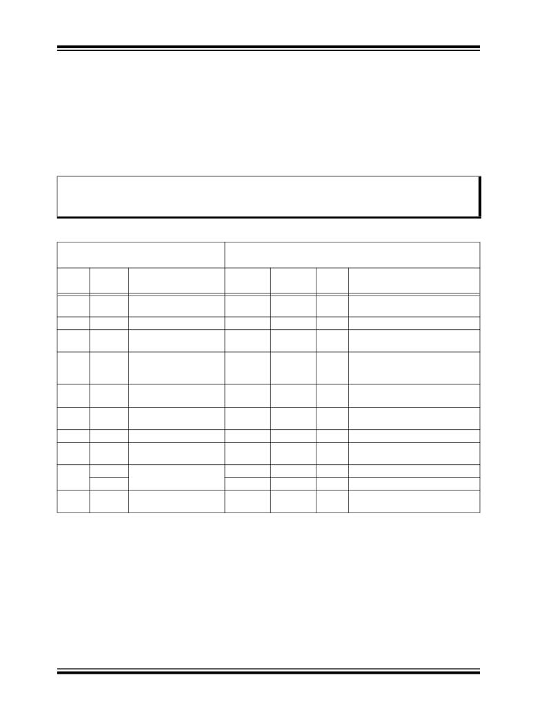
TABLE 1-1:
DC CHARACTERISTICS
DC CHARACTERISTICS
Industrial (I): V CC = +1.7V to 5.5V T A = -40°C to +85°C
Automotive (E): Vcc = +2.5V to 5.5V T A = -40°C to +125°C
Param.
No.
Sym.
—
Characteristic
A1, A2, SCL, SDA and
Min.
—
Max.
—
Units
—
Conditions
WP pins:
D1
V IH
High-level input voltage
0.7 V CC
—
V
D2
V IL
Low-level input voltage
—
0.3 V CC
V
V CC ?? 2.5V
0.2 V CC
V
V CC < 2.5V
D3
V HYS
Hysteresis of Schmitt
0.05 V CC
—
V
V CC ? 2.5V ( Note )
Trigger inputs
(SDA, SCL pins)
D4
V OL
Low-level output voltage
—
0.40
V
I OL = 3.0 mA @ V CC = 4.5V
I OL = 2.1 mA @ V CC = 2.5V
D5
I LI
Input leakage current
—
±1
? A
V IN = V SS or V CC
V IN = V SS or V CC
D6
D7
I LO
C IN ,
Output leakage current
Pin capacitance
—
—
±1
10
? A
pF
V OUT = V SS or V CC
V CC = 5.0V ( Note )
C OUT
(all inputs/outputs)
T A = 25°C, F CLK = 1 MHz
D8
I CC Read Operating current
I CC Write
—
—
450
5
? A
mA
V CC = 5.5V, SCL = 400 kHz
V CC = 5.5V
D9
I CCS
Standby current
—
5
? A
SCL, SDA, V CC = 5.5V
A1, A2, WP = V SS
Note:
This parameter is periodically sampled and not 100% tested.
DS22270C-page 2
? 2011-2012 Microchip Technology Inc.
发布紧急采购,3分钟左右您将得到回复。
相关PDF资料
24FC128-I/MNY
IC EEPROM 128KBIT 1MHZ 8TDFN
24FC515T-I/SM
IC EEPROM 512KBIT 1MHZ 8SOIC
24FC64T-I/MF
IC EEPROM 64KBIT 1MHZ 8DFN
24LC014H-I/P
IC EEPROM 1KBIT 400KHZ 8DIP
24LC014T-E/OT
IC EEPROM 1KBIT 400KHZ SOT23-6
24LC01B-I/SNG
IC EEPROM 1KBIT 400KHZ 8SOIC
24LC024H-I/ST
IC EEPROM 2KBIT 400KHZ 8TSSOP
24LC025T-E/MC
IC EEPROM 2KBIT 400KHZ 8DFN
相关代理商/技术参数
24FC1026-I/SM
功能描述:电可擦除可编程只读存储器 1024K 128K X 8 2.5V HI-SPD EE 128BYTE PG RoHS:否 制造商:Atmel 存储容量:2 Kbit 组织:256 B x 8 数据保留:100 yr 最大时钟频率:1000 KHz 最大工作电流:6 uA 工作电源电压:1.7 V to 5.5 V 最大工作温度:+ 85 C 安装风格:SMD/SMT 封装 / 箱体:SOIC-8
24FC1026-I/SN
功能描述:电可擦除可编程只读存储器 1024K 128K X 8 2.5V HI-SPD EE 128BYTE PG RoHS:否 制造商:Atmel 存储容量:2 Kbit 组织:256 B x 8 数据保留:100 yr 最大时钟频率:1000 KHz 最大工作电流:6 uA 工作电源电压:1.7 V to 5.5 V 最大工作温度:+ 85 C 安装风格:SMD/SMT 封装 / 箱体:SOIC-8
24FC1026-I/ST
功能描述:电可擦除可编程只读存储器 1024K 128K X 8 2.5V HI-SP SER EE 128BYTE RoHS:否 制造商:Atmel 存储容量:2 Kbit 组织:256 B x 8 数据保留:100 yr 最大时钟频率:1000 KHz 最大工作电流:6 uA 工作电源电压:1.7 V to 5.5 V 最大工作温度:+ 85 C 安装风格:SMD/SMT 封装 / 箱体:SOIC-8
24FC1026T
制造商:MICROCHIP 制造商全称:Microchip Technology 功能描述:1024K I2C? CMOS Serial EEPROM 100 kHz and 400 kHz Clock Compatibility
24FC1026T-I/SM
功能描述:电可擦除可编程只读存储器 1024K 128K X 8 2.5V HI-SPD EE 128BYTE PG RoHS:否 制造商:Atmel 存储容量:2 Kbit 组织:256 B x 8 数据保留:100 yr 最大时钟频率:1000 KHz 最大工作电流:6 uA 工作电源电压:1.7 V to 5.5 V 最大工作温度:+ 85 C 安装风格:SMD/SMT 封装 / 箱体:SOIC-8
24FC1026T-I/SN
功能描述:电可擦除可编程只读存储器 1024K 128K X 8 2.5V HI-SPD EE 128B PAGE RoHS:否 制造商:Atmel 存储容量:2 Kbit 组织:256 B x 8 数据保留:100 yr 最大时钟频率:1000 KHz 最大工作电流:6 uA 工作电源电压:1.7 V to 5.5 V 最大工作温度:+ 85 C 安装风格:SMD/SMT 封装 / 箱体:SOIC-8
24FC1026T-I/ST
功能描述:电可擦除可编程只读存储器 1024K 128K X 8 2.5V HI-SP SER EE 128BYTE RoHS:否 制造商:Atmel 存储容量:2 Kbit 组织:256 B x 8 数据保留:100 yr 最大时钟频率:1000 KHz 最大工作电流:6 uA 工作电源电压:1.7 V to 5.5 V 最大工作温度:+ 85 C 安装风格:SMD/SMT 封装 / 箱体:SOIC-8
24FC128
制造商:MICROCHIP 制造商全称:Microchip Technology 功能描述:128K I2C CMOS Serial EEPROM
